Hardware Quick Reference
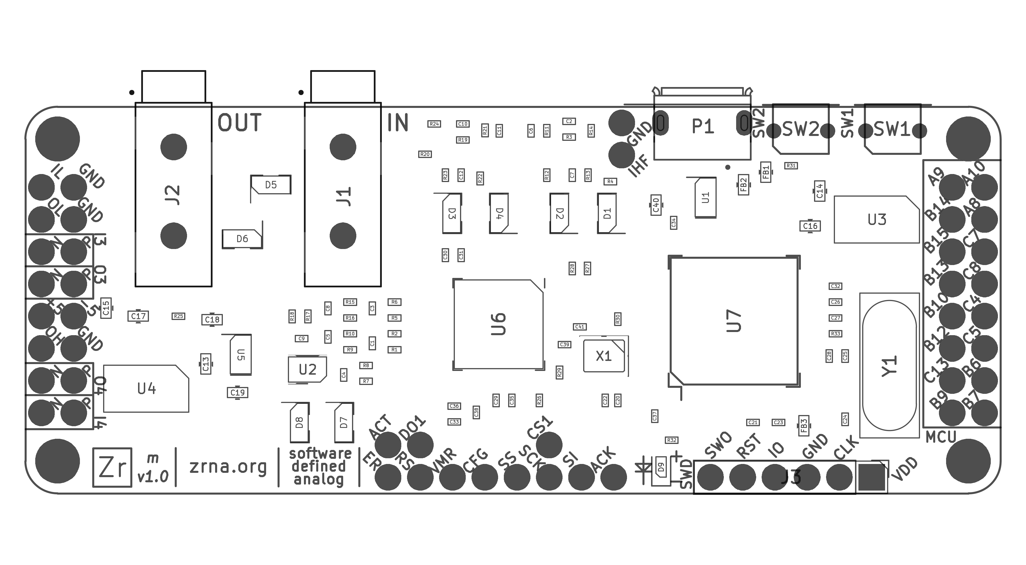
Test Point Pinout
$$ \text{MCU IO (PCB Right Edge)} \\ \begin{array}{|c|c|c|} \hline \text{Label} & \text{Default Function} & \text{API Requests?}\\ \hline \text{A9} & \text{USART1 TX} & \text{Yes}\\ \hline \text{A10} & \text{USART1 RX} & \text{Yes}\\ \hline \text{B14} & \text{SPI2 MISO} & \text{Yes}\\ \hline \text{A8} & \text{PA8 GPIO} & \\ \hline \text{B15} & \text{SPI2 MOSI} & \text{Yes}\\ \hline \text{C7} & \text{PC7 GPIO} & \\ \hline \text{B13} & \text{SPI2 SCK} & \text{Yes}\\ \hline \text{C8} & \text{PC7 GPIO} & \\ \hline \text{B10} & \text{I2C2 SCL} & \text{Yes}\\ \hline \text{C4} & \text{ADC1 IN4} & \\ \hline \text{B12} & \text{SPI2 NSS} & \text{Yes}\\ \hline \text{C5} & \text{ADC1 IN5} & \\ \hline \text{C13} & \text{PC13 GPIO} & \\ \hline \text{B6} & \text{I2C1 SCL} & \\ \hline \text{B9} & \text{I2C2 SDA} & \text{Yes}\\ \hline \text{B7} & \text{I2C1 SDA} & \\ \hline \end{array} \\ $$
The MCU IO labels above correspond to the pin labels for the STM32F413 processor. The default configuration exposes UART, SPI and I2C for API communications, but each pin has several possible functions assignable in software. See the datasheet below for the complete pin mapping.
$$ \text{FPAA IO (PCB Left Edge)} \\ \begin{array}{|c|c|c|} \hline \text{Label} & \text{Function} & \text{Range} & \approx\text{Bandwidth} \\ \hline \text{IL, GND} & \text{Audio Input} & \text{-5V to +5V} & \lt \text{24kHz}\\ \hline \text{OL, GND} & \text{Audio Output} & \text{-5V to +5V} & \lt \text{24kHz}\\ \hline \text{N, P (I3)} & \text{Diff. Input Cell 3} & \text{0-3V, centered at 1.5V}& \lt \text{2MHz}\\ \hline \text{N, P (O3)} & \text{Diff. Output Cell 3} & \text{0-3V, centered at 1.5V}& \lt \text{2MHz}\\ \hline \text{+5, -5} & \text{+5V and -5V Rails} & \text{Const.} & \text{DC}\\ \hline \text{OH, GND} & \text{Ultrasonic Output} & \text{-5V to +5V} & \lt \text{2MHz}\\ \hline \text{N, P (I4)} & \text{Diff. Input Cell 4} & \text{0-3V, centered at 1.5V}& \lt \text{2MHz}\\ \hline \text{N, P (O4)} & \text{Diff. Output Cell 4} & \text{0-3V, centered at 1.5V}& \lt \text{2MHz}\\ \hline \end{array} \\ $$ $$ \text{FPAA IO (PCB Center Top)} \\ \begin{array}{|c|c|c|} \hline \text{Label} & \text{Function} & \text{Range} & \approx\text{Bandwidth} \\ \hline \text{IHF, GND} & \text{Ultrasonic Input} & \text{-5V to +5V} & \lt \text{2MHz}\\ \hline \end{array} \\ $$ $$ \text{FPAA IO (PCB Center Bottom)} \\ \begin{array}{|c|c|} \hline \text{ACK} & \text{16Mhz Clock} \\ \hline \text{SI} & \text{SPI MOSI from MCU to FPAA} \\ \hline \text{SCK} & \text{SPI Clock from MCU to FPAA} \\ \hline \text{SS} & \text{SPI NSS from MCU to FPAA} \\ \hline \text{CS1} & \text{FPAA CS1b} \\ \hline \text{CFG} & \text{FPAA CFGFLGb} \\ \hline \text{VMR} & \text{FPAA VMR} \\ \hline \text{RS} & \text{FPAA RESETb} \\ \hline \text{DO1} & \text{FPAA LCCb/Digital Output} \\ \hline \text{ER} & \text{FPAA ERRb} \\ \hline \text{ACT} & \text{FPAA ACTIVATE} \\ \hline \end{array} \\ $$Connectors and Switches
$$ \begin{array}{|c|c|c|} \hline \text{J1} & \text{3.5mm Audio Input, +5/-5V rails} \\ \hline \text{J2} & \text{3.5mm Audio Output, +5/-5V rails} \\ \hline \text{P1} & \text{Micro USB, Power and Data} \\ \hline \text{SW2} & \text{Hold on startup to enter DFU mode.} \\ \hline \text{SW1} & \text{Device reset. Hold on startup to enter bootloader.} \\ \hline \end{array} \\ $$
Datasheets
STM32F413RGTx: ARM Cortex M4F microcontroller
AN231E04: field-programmable analog array