165ctrl v
external digital input pin control v version: variable rate control
Inlets
None
Outlets
None
Attributes
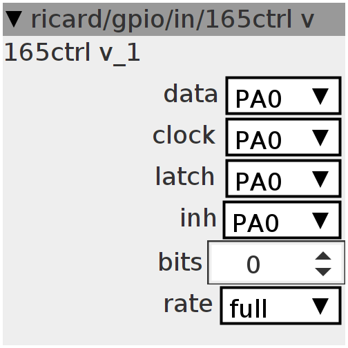
combo pin for data input
combo pin for clock output
combo pin for latch output
combo pin for inh output
combo how much of the read loop is done at one time
spinner number of bits to shift in
Declaration
unsigned int data;  // data output
unsigned int rdata; // internal data read
int count;
int looprate;
Init
palSetPadMode(attr_data, PAL_MODE_INPUT);
palSetPadMode(attr_clock, PAL_MODE_OUTPUT_PUSHPULL);
palSetPadMode(attr_latch, PAL_MODE_OUTPUT_PUSHPULL);
palSetPadMode(attr_inh, PAL_MODE_OUTPUT_PUSHPULL);
palWritePad(attr_inh, 0);   // inhibit, leave 0 at all times to enable clock
palWritePad(attr_latch, 1); // parallel load when 0 (level sensitive)
palWritePad(attr_clock,
            1); // clock data on rising edge, must be high during parallel load
data = 0;
rdata = 0;
count = -2;
Control Rate
// Sequence: count runs from -2 to attr_bits<<1 - 1
// For -2 and -1, pulse latch (parallel load) low, must be high afterwards.
// for 0..attr_bits<<1 - 1, read data bit, then pulse clock low.
// Data is shifted on the rising edge of the clock, and the clock must
// remain high after reading so that it is high during the parallel
// load phase (see HC165 data sheet).
looprate = ((attr_bits << 1) + 2) / attr_rate;
if (!looprate)
  looprate = 1;
for (int i = 0; i < looprate; i++) {
  if (count < 0) {
    palWritePad(attr_latch,
                count & 1); // pulse low, then leave high for readout
    count++;
  } else {
    if (count & 1) {
      if (palReadPad(attr_data))
        rdata |= 1 << (count >> 1);
      else
        rdata &= ~(1 << (count >> 1));
    }
    palWritePad(attr_clock, count & 1);
    count++;
    if (count > (attr_bits << 1) - 1) {
      count = -2;
      data = rdata; // set all bits in output word at once
      // clock is left high for next latch pulse (see 165 data sheet truth
      // table)
    }
  }
}